A New Design Technique for a HighSpeed Circuit Diagram A logic level shifter, or a voltage level translator, is used to translate signals from one logic level to another. Nowadays, most of the system runs on 3.3V or 5V. Logic level is simply a HIGH and LOW level of voltage for a certain board or IC. Design a 5V to 3.3V Translation Circuit. To translate 5V signals to 3.3V signals, the simplest So R1 and R2 form a voltage divider, and R2 should be twice R1 to get the 0 V. Next we have to find the amplification, which is determined by R3 and R4: (the "to_adc" is the output voltage): The above non-inverting circuit is a bit like your summing amplifier. (e.g. > 5k) you will need to buffer the signal before sending to the level The simplest and most common method of logic level shifting is a voltage divider. In the circuit shown as in the first picture, the output of the divider is the line coming out from the middle. There is a total of 5V dropped across the circuit, but we can can calculate how much voltage is dropped across each resistor.

A level shifter is an electronic device that changes the voltage level of signals between different logic circuits or microcontrollers. The main purpose of using a level shifter is to ensure compatibility between components that Level Shifter Circuits - Design Basics and Applications R19WP0010EU0100 Rev.1.00 Jul 11, 2024 Page 9 4. Conclusion It may get damaged, so we need logic level shifter. Let's make a simple logic level shifter using two npn transistors. These types of level shifter are widely use in many of the digital devics. In this instructables we are going to design a simple circuit of level shifter just for understanding how they works. Practically cmos are preferred for

A Quick Guide on Logic Level Shifting Circuit Diagram
In the logic level shifter circuit shown above, consider that the MOSFET turns on fully when we supply a Gate-Source voltage (V GS) of 3.3 Volts. Low-level to high-level conversion: When the voltage at point A is at 3.3V, the MOSFET stays in the cut-off region as the voltage difference between the Gate and Source is less than the threshold voltage signals themselves, requiring a level-shifter and hence high voltage switch control on their own. This is accomplished with two cross-coupled circuits like those shown in Fig. 4 where each cell provides the high voltage switch signals of the other. B. Complete level-shifter circuit From the timing diagram in Fig. 4 it is evident that the

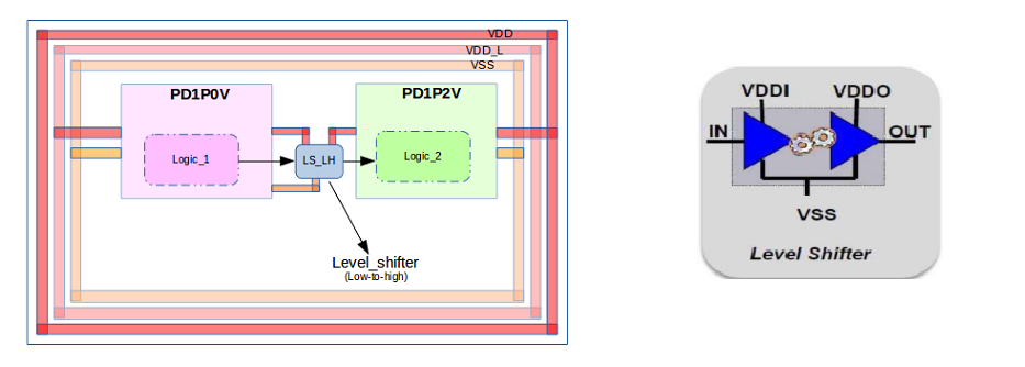
A level shifter circuit is used to convert signals from one voltage level to another while maintaining the shape of the signal. This is commonly needed when interfacing different parts of a system that operate at different voltage levels, such as between microcontrollers, sensors, or other integrated circuits.